Archived Research Projects
Research projects that are a bit older have been moved to this page. We're not saying you're old - just kind of marinated.
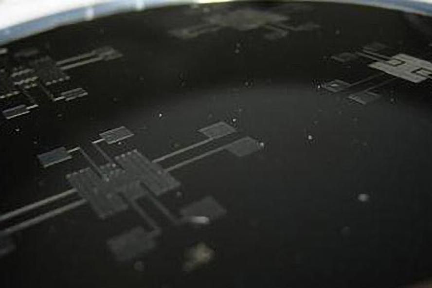
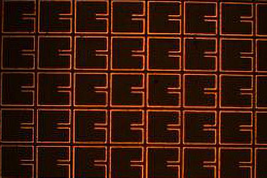
THz and Millimeterwave Metamaterials
The THz and millimeterwave metamaterials are fabricated successfully at wafer scale on flexible substrates. The metamaterials are fabricated on different flexible substrates using standard deep UV photolithography patterning, gold metalization and liftoff process. The critical dimension is 15 um.
Postdoc: Pramod Singh, ECE
Advisor: Professor Sameer Sonkusale, ECE
Floating Element Surface Shear Sensors
Floating element surface shear force sensors are under development for aerospace applications. These sensors detect surface shear by measuring a capacitance change for a deflecting shuttle. The sensors under development include active feedback control for rebalancing of the shuttle in an effort to extend dynamic range, reduce nonlinearities, and reject disturbances. With Spirit Aerosystems.
Student: Zhengxin Zhao, ME PhD student
Advisor: Professor Robert White, Mechanical Engineering
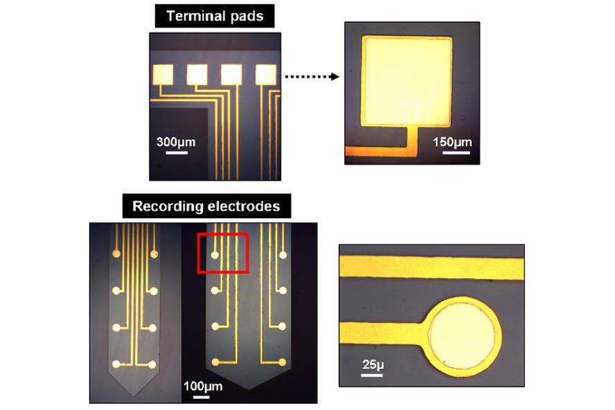
Flexible Parylene-based Microelectrode Arrays
A flexible multi-electrode array intended for high resolution electromyographic (EMG) recordings has been fabricated using Parylene C as substrate material. The fabrication protocol comprises vapor deposition of parylene C, standard photolithography, sputtering deposition and reactive ion etching. The thickness of the final devices is <20μm, while the radius of the recording electrodes is 40μm. The devices have been successfully tested in vivo in the model system Manduca sexta.
Student: Cinzia Metallo, Neuroscience PhD student
Advisor: Professor Barry Trimmer, Biology
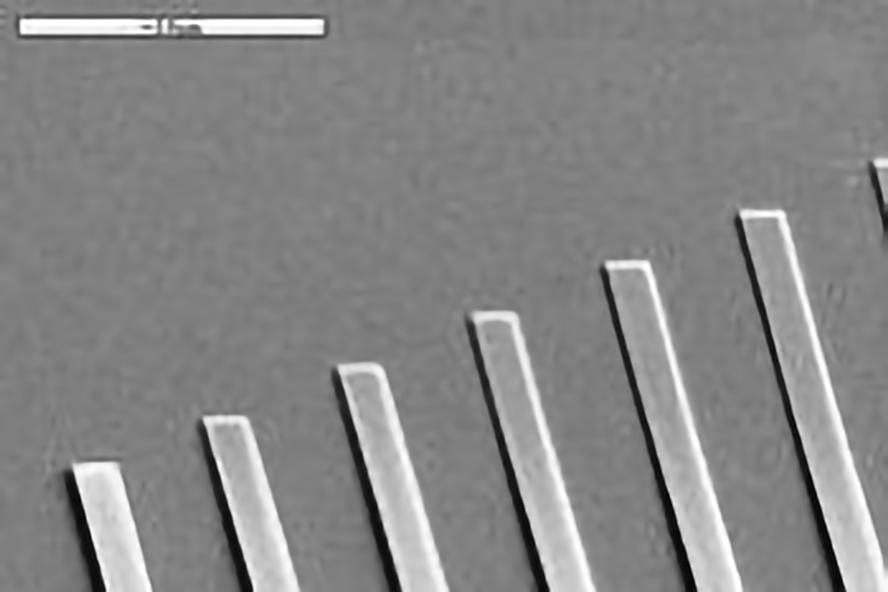
Hair-like Surface Shear Force Sensors
MEMS shear sensor and shear sensor arrays for surface shear force measurement are under development. The shear sensor consists of 80 µm high SU-8 posts resting on a polysilicon base. A capacitive sensing scheme is used for detecting the vector force applied to this post. Different size hair-sensors and hair-sensor layouts are designed. The sensitivity and dynamic range of each design are computed. Predicted dynamic range is on the order of 60 dB. The most sensitive design is expected to measure shear forces on the order of 0.1 Pa in a 500 Hz band. Fabrication combines the polyMUMPS foundry process with post-processing at Tufts. Characterization is ongoing. Major support from Spirit Aerosystems with additional funding from NASA and DARPA.
Student: Shuangqin Liu, ME PhD student
Advisor: Professor Robert White, ME
Microscope picture of the hair sensor arrays. These are 80 micron high posts with all the associated capacitive readouts.
Copper Nanowires for Crossed-Nanowire Transistors
Copper nanowires (with a thin copper oxide sheath) were grown on a silver substrate for use as the gate in experimental crossed-nanowire transistors. The nanowires are grown by the electroplating of copper through anodized aluminum templates, which were later etched. The nanowires are ~150nm in diameter and 5um in length. Other potential applications include anodes in super-capacitors, frictional elements, and high surface area electrodes for sensing.
Student: Sam MacNaughton, ECE MS student
Advisor: Professor Sameer Sonkusale, ECE
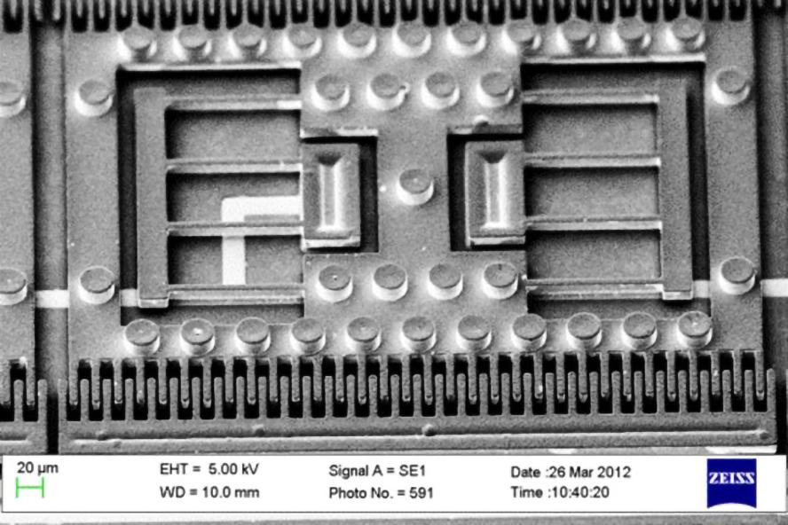
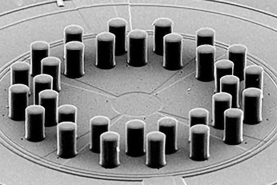
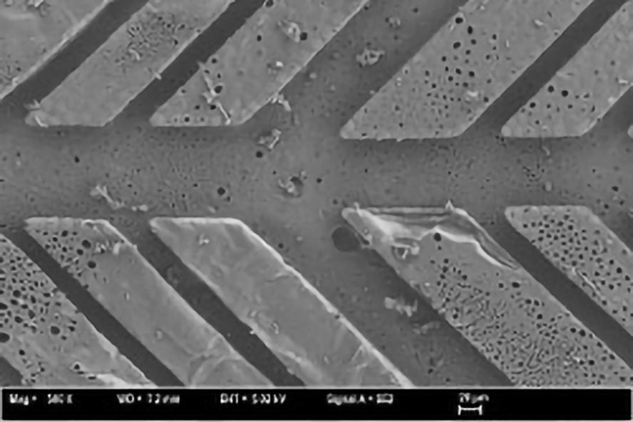
Micromachined Pressure Sensor Arrays for Aeroacoustics
Design, fabrication, and characterization of a surface micromachined, front-vented, 64 channel (8X8), capacitively sensed pressure sensor array is underway. The array was fabricated using the MEMSCAP PolyMUMPs process, a three layer polysilicon surface micromachining process with additional postprocessing fabrication steps (release, packaging, Parylene coating) carried out at Tufts. Acoustic sensitivity studies show single element acoustic sensitivity of 0.7 mV/Pa from 200 to 20 kHz.
Student: Joshua Krause, ME PhD student
Advisor: Professor Robert White, ME
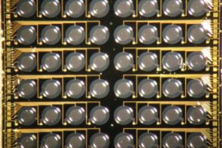
Light microscope image of the array. The elements are made of 3.5 micron thick polysilicon with a 2 micron air gap to the bottom electrode.
SEM image of a single element. The wires (and writing) are Cr/Au on polysilicon. Element diameter is 0.6 mm and pitch is 1.3 mm.
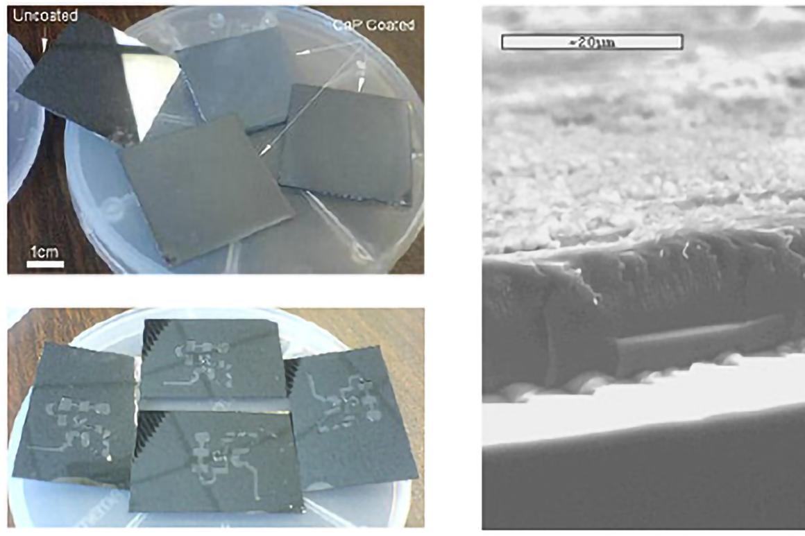
Lab-on-a-chip Devices for Dynamic Seeding of Bone Cells
Lab-on-a-chip devices have become increasingly popular as quick and easy diagnostic and experimental tools due to their size, flexibility in application, and relative ease of manufacturing and use. The development of customizable lab-on-a-chip features, such as surface patterning or coatings, can have widespread application. This research established low-cost and simple calcium phosphate coating capabilities on a silicon wafer using electrophoretic deposition, as well as the ability to pattern such a coated wafer with photoresist. The coated and patterned wafer was used to evaluate the ability of bone cells to adhere to a microchannel surface under flow, or dynamic seeding conditions.
Student: Erica Belmont, ME MS student
Advisor: Professor Douglas Matson, ME
Micromolding of Aqueous-Derived Silk Structures
There is enormous potential for biopolymers in MEMS applications. In MEMS devices biopolymers could function as membranes or optical components. Devices which demand outstanding biocompatibility, such as implantable sensors, could be packed in or fully manufactured from biopolymers materials. The challenge today exists in understanding critical processing parameters in manufacturing structures with micron and submicron level features from biopolymers. In this research, the development of a micromolding technology, to produce microstructures from aqueous derived silk solutions is studied. In particular, well-defined cellular and tissue culture substrate (scaffold) fabrication is used as a model to study manufacturing methods. The manufacturing challenges consist in counteracting shrinkage caused by solvent evaporation, producing well defined porous structures and demolding of delicate structures.
Student: Konstantinos Tsioris, ME MS student
Advisor: Professor Wong, ME
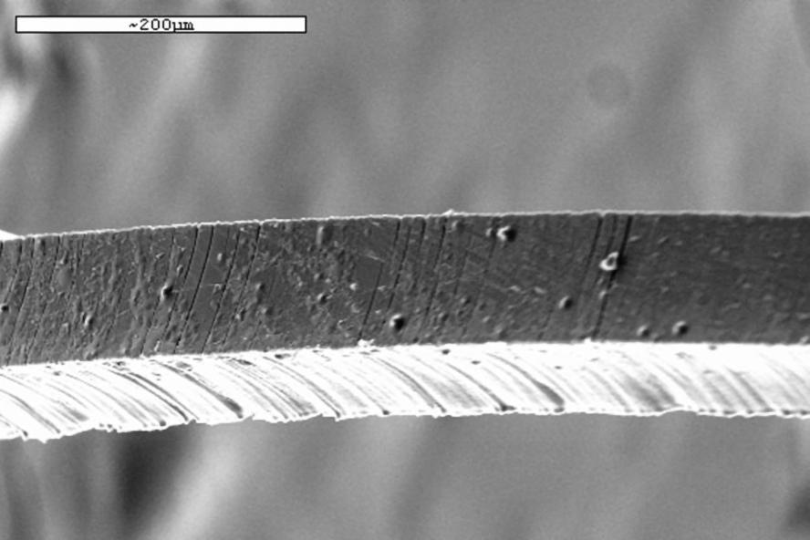
SEM image of silk fiber (crossection 100 x 100 µm) as part of well defined scaffold layer.
PDMS microchannel system (individual channels: width 100 µm x height 250 µm) produced with SU-8 photolithography.
Microfabricated Perfusion System for Vascularized Tissues
There is a critical clinical demand for tissue-engineered, three-dimensional constructs for tissue repair and organ replacements. Upon initial implantation, three-dimensional (3-D), tissue-engineered (TE) constructs maintain functionality and interface with the human body. In the long-term, however, necrosis occurs at the core of the construct because of limited oxygen and nutrient diffusion into the deeper layers of the TE construct. The diffusion limit of oxygen and nutrients into 3-D TE constructs is a major obstacle in the tissue engineering field. The clinical success of future 3-D TE constructs depends on developing the capability to deliver nutrients to larger systems.
Student: Lindsay Wray, BME PhD student
Advisor: Professor David Kaplan, BME
SEM images of microchannels molded into a porous silk fibroin scaffold.
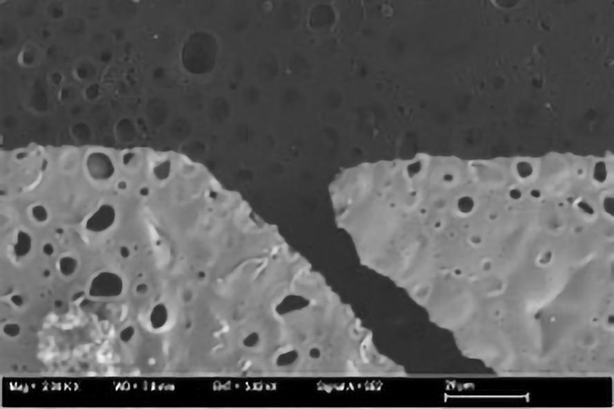
Channels have widths ranging from 25 um to 300 um and depths ranging from 10 um to 150 um. The microchannel pores are on average 2 um in diameter.
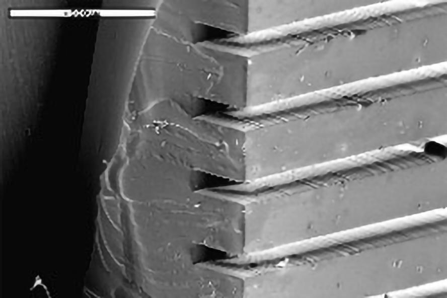
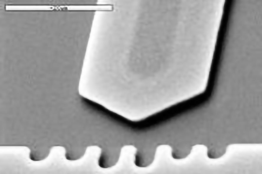
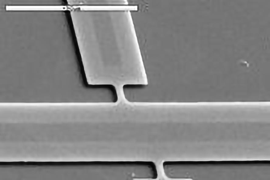
Comparison of Techniques for Polysilicon Residual \ Stress Measurements
Experimental work comparing wafer curvature measurements, micro-rotating structures, buckling microstructures, and vibrating microstructures for the measurement of residual stresses in thin polysilicon films.
Student: Andrew Mueller, ME Masters of Science student
Advisor: Professor Robert White, ME
Pictured below: SEM images of surface-micromachined polysilicon structures developed at Tufts by Andrew Mueller and Robert White. Fabrication was conducted partly at the Tufts Microfab, partly at the MIT Microsystems Technology Laboratory and partly at the University of Michigan Nanofabrication Facility.
Calibration Targets for Dual Emission Laser Induced Fluorescence (DELIF)
Calibration wafers have been fabricated to calibrate an optical measurement technique called Dual Emission Laser Induced Fluorescence (DELIF), which is used to determine fluid film thickness between a glass wafer and a polishing pad during Chemical Mechanical Polishing (CMP). Square wells measuring 1mm2 and 0.25mm2 are etched into these glass wafers to known depths (up to 130um). The necessary well etch depth depends on the surface roughness of the polishing pad. In order for fluid layer thickness difference under the wells to be detectable, the well depth should be at least 3 times the surface roughness of the pad.
Student: Caprice Gray, ME PhD student
Advisors: Professor Chris Rogers, Professor Robert White, ME
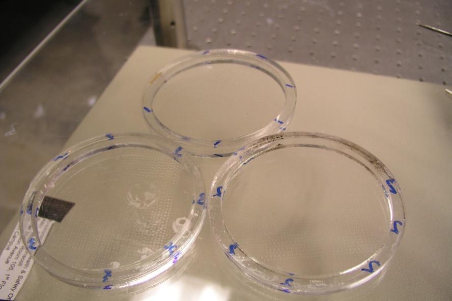
Photograph of etched glass calibration wafers used to determine thin fluid film thickness during DELIF.
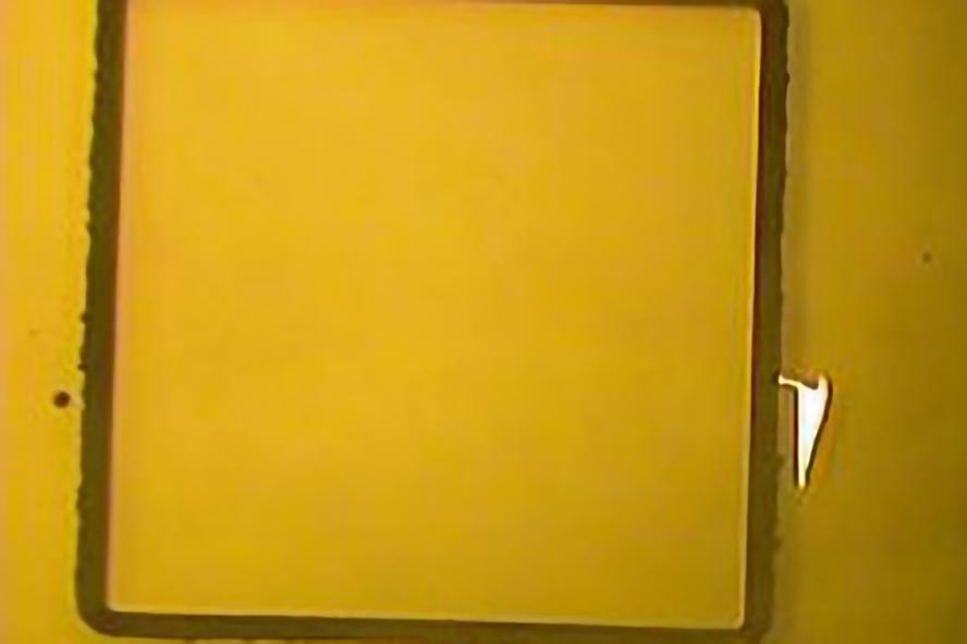
A light microscope picture of a single 1mm2 calibration well 23 microns deep.
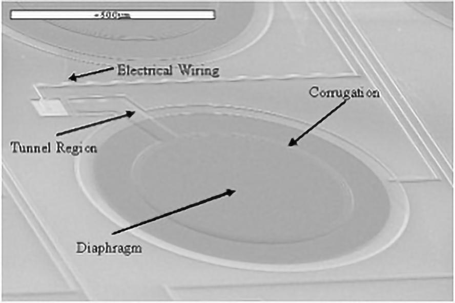
Micromachined Shear Stress Sensors for in-situ Monitoring of Surface Forces in ChemiMechanical Planarization
A PDMS microstructure is being developed to measured the interaction forces that occur between a wafer and a polishing pad during CMP. The PDMS structures deflect in response to fluid forces and solid-solid contact forces. An optical method is used to monitor structure deflection in-situ.
Student: Minchul Shin, ME PhD student, Doug Gauthier and Andrew Mueller, ME Masters of Science students
Advisor: Professor Robert White, ME
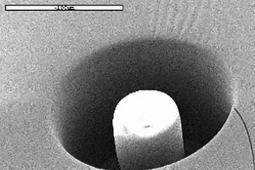
SEM image 30 micron diameter, 100 micron tall PDMS post-in-well developed for the CMP shear stress sensor project.
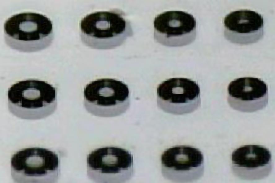
Angled light microscope picture showing a portion of the array with different sized PDMS posts-in-wells.
Thermal Design and Fabrication of Microscale Heaters
Microscale heaters with integrated thermistors were fabricated as an undergraduate research project. The devices use thin sputtered nickel films for both heating and sensing elements. The processes involved were standard photolithography, sputtering, and liftoff. Some of the heaters were functional, and some failed. Residual stresses, particles, and/or human error in processing appear to have caused the observed defect in some of the heater lines.
Student: Michael Rizzolo, ME undergraduate
Advisor: Professor Wong, ME